The demands of the “Performance × Power × Area” (PPA) pose a diverse challenge to the future integrated circuits (ICs). Thus, the aggressive evolution of the feature size and shrinking of technology nodes of IC manufacturing have been gradually abandoned, by substituted with the development on three-dimensional (3D) integration technology of transistors and circuits. By comparison to the advanced 3D packaging with a mature market, monolithic 3D (M3D) integration technology promises a theoretical higher density of interlayer connections and transistors, based on the front end of line (FEOL) and the back end of line (BEOL) manufacturing. The temperature of fabrication flow for upper-layer transistors is forced to cut down considering the thermal budget in previous silicon based M3D researches, leading to a lower performance and falling behind planar silicon advanced nodes. High-density and high-purity carbon nanotube (CNT) arrays promise a low-temperature method for channel materials preparation and transistors fabrication, which is beneficial for compatible M3D processing. Besides, the M3D structure contributes to reduce the total wire length and speed up the carbon-based ICs. (Nano Res. 2019;12(8):1810) Therefore, CNT FET is suitable for constructing the high-speed M3D ICs. But there lacks the robust interlayer technology and high-quality upper-layer channel materials to date, which restricts the performance of M3D devices and ICs.
The research group of Prof. Zhiyong Zhang (
School of Electronics; Research Center for
Carbon-Based Electronics; Key Laboratory for the Physics and Chemistry of Nanodevices and Center for Carbon-based Electronics, Peking University
), collaborated with the research group of Prof. Chuanhong Jin (School of Materials Science and Engineering, Zhejiang University) have been studying on the key technology of aligned CNT based M3D. A high-quality interlayer technology with high planarization, low surface roughness (Ra<0.5 nm) and low-k (~3) is realized by spin-on-glass (SOG) materials, boosting the fine-grain M3D integrated CNT FET with the interlayer alignment of 20 nm. (Fig. 1a-1d) The bottom-layer A-CNT FETs with the Lg of 90 nm and the Vds of -0.7 V show an ultrahigh on-state performance with the Ion of 1.84 mA/μm and the peak gm of 1.65 mS/μm, which exceeds the gm performance of 45 nm-node Si PMOS FET. (Fig. 2a-2c) Based on the highly-oriented transfer method at low temperature, A-CNT materials can be prepared on the surface of SOG, exhibiting a field-effect carrier mobility of 650 cm2/Vs. The upper-layer A-CNT FETs are fabricated by low-temperature processes meeting the bottom-layer stability. The on-state current density of upper-layer CNT FETs surpass the upper-layer transistors in other M3D research works of silicon, OFET and 2D materials, et al. (Fig. 3a-3d) Furthermore, the group realize the demonstrations of high-speed CNT M3D ICs. The M3D 5-stage ring oscillators (ROs) with active area of 100 μm2 are fabricated and can output the highest oscillating frequency of 5.78 GHz, that is, the delay per stage of 17 ps (Fig. 4a-4d), represents the most compact and fastest 3DICs to date. (Fig. 5a-5b)
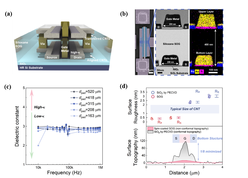
Fig. 1 High-quality interlayer technology; M3D integrated CNT FETs.
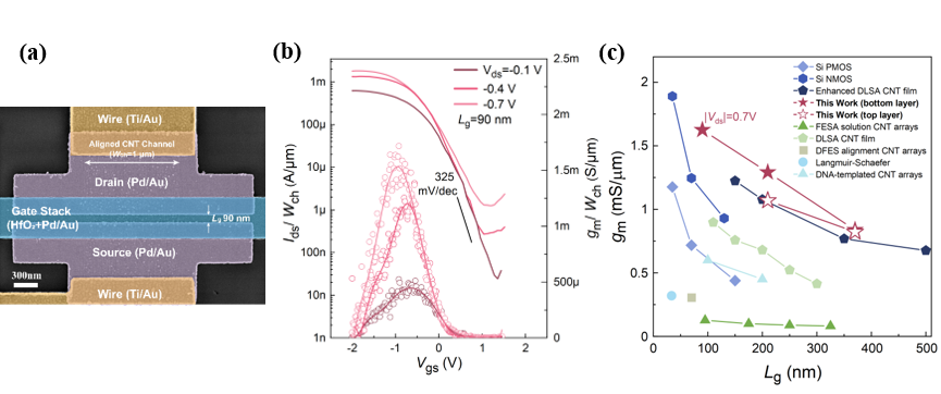
Fig. 2 Characteristics of bottom-layer high-performance CNT FETs.
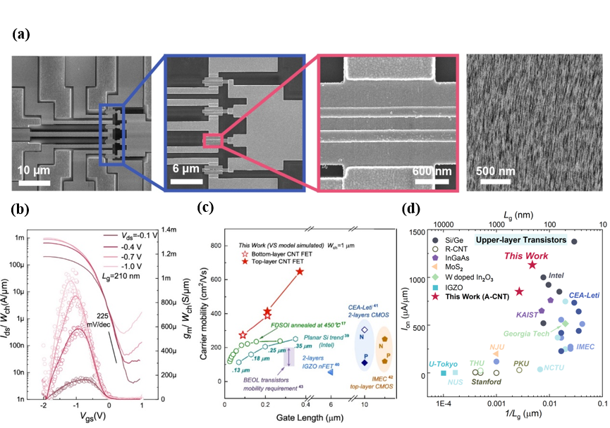
Fig. 3 Characteristics and benchmarks of upper-layer CNT FETs.
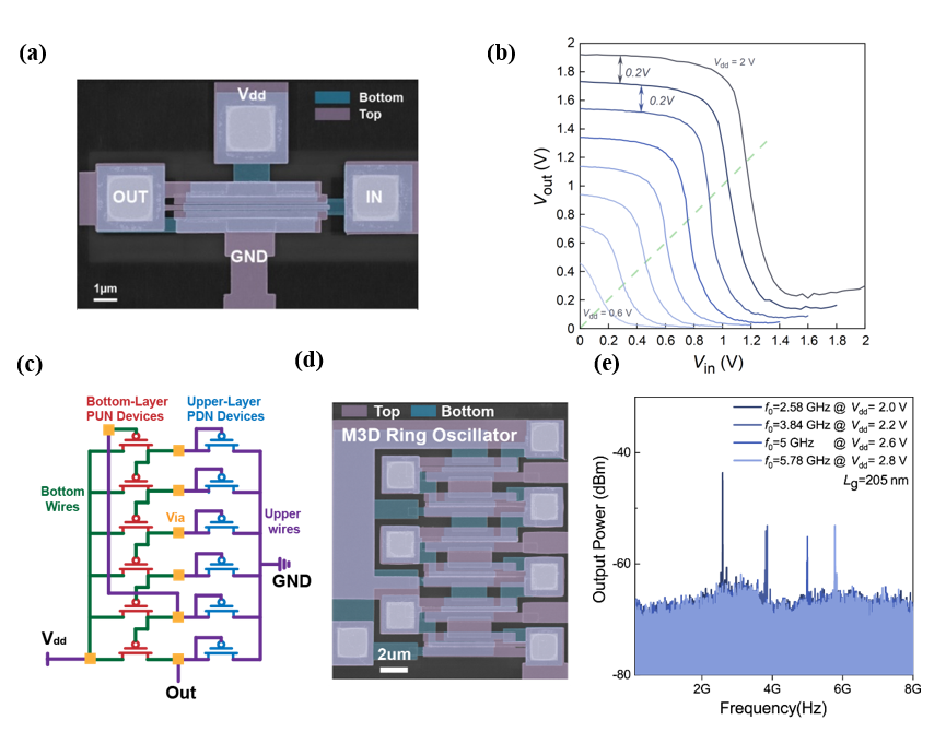
Fig. 4 Characteristics of M3D inverters and M3D 5-stage ring oscillators.
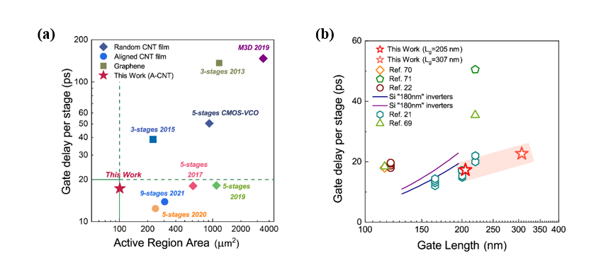
Fig. 5 Benchmarks for Speed×Area index of CNT M3D ROs.